Electronics Manufacturing

GlobalFoundries Names Vermont GaN Hub in $16B US Expansion

Image
GlobalFoundries Names Vermont GaN Hub in $16B US Expansion

New York – October 26, 2026 -- GlobalFoundries (GF) has committed $16 billion to expand manufacturing and advanced packaging in New York and Vermont, and has designated its Vermont site as the core hub for gallium nitride (GaN) technology development. The October 26, 2026 announcement is backed by Apple, SpaceX, AMD, Qualcomm, NXP and General Motors.

The plan also covers silicon photonics for data centers and FDX processes for edge AI. One month after the announcement, TSMC confirmed it will exit the GaN foundry business by 2027, which leaves a gap in the market for a domestic alternative.


ARM Readies First In-House Chip as Intel Strategy Faces Doubt

Image
ARM Readies First In-House Chip as Intel Strategy Faces Doubt

Global – October 26, 2026 -- ARM is set to debut its first in-house chip by summer, moving beyond its traditional role as an IP provider into chip design, while Intel's strategy as an integrated device manufacturer (IDM) faces questions after CEO Pat Gelsinger departed in December 2024.

ARM and Intel shifts reshape a value chain split into eight segments

The semiconductor value chain spans IP design, electronic design automation (EDA), fabless design, foundries and outsourced assembly and test (OSAT), IDMs, chemical and wafer suppliers, equipment makers, and the manufacturers that integrate chips into end products. No single country or company controls every stage. Emerging players backed by substantial government funding are working to close the technology gap, and startups are investing in specialized areas that could disrupt the industry's traditional dynamics.

GlobalFoundries Moves RF GaN to Volume, Cuts RF Die Area 45%

Image
GlobalFoundries Moves RF GaN to Volume, Cuts RF Die Area 45%

Burlington – October 25, 2026 -- GlobalFoundries (GF) has qualified RFGaN1, its first RF GaN-on-silicon technology for volume production on 200mm wafers. It has also qualified SLATE, a wafer-bonding technology that cuts RF die area by up to 45% with no loss in RF performance.

RFGaN1 runs at 12 to 28V across 1 to 15 GHz

The platform uses depletion-mode devices and targets sustained high output power and efficiency in satellite communications, cellular infrastructure and defense. Dan Denninghoff, Senior Director of RF GaN Product Line, said GaN has so far been a niche, high-budget option. GF argues that 200mm silicon manufacturing gives customers the cost structure and volume to build a supply chain around it instead of treating each design as a one-off.

Hormuz Closure Threatens Chip Output via Helium, Bromine Shortages

Image
Hormuz Closure Threatens Chip Output via Helium, Bromine Shortages

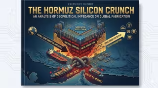
Middle East – October 25, 2026 -- Spot helium prices have doubled after Iranian strikes hit Qatar's Ras Laffan Industrial City, exposing semiconductor fabs to a materials shortage that extends well beyond oil.

Qatar produced roughly one-third of the world's helium as a byproduct of LNG processing. QatarEnergy has declared force majeure, and repairs are estimated at three to five years.

Stranded cryogenic containers put a 35-to-48-day clock on Asian fabs

Roughly 200 specialised cryogenic containers are stranded near the Strait of Hormuz. They keep helium liquid for only 35 to 48 days before it warms and escapes. The last scheduled shipments to Asian fabs are arriving now.

Chip Market Targets $1 Trillion by 2030-2032 Across Global Chain

Image
Chip Market Targets $1 Trillion by 2030-2032 Across Global Chain

Global – October 25, 2026 -- The semiconductor industry is projected to reach a market value of $1 trillion by 2030-2032, built on a production chain that spans several continents and thousands of precision steps.

Wafer size of 300mm dominates modern fabrication for higher chip yield

Production starts with refining sand into ultra-pure silicon, the second most abundant element in Earth's crust at about 28%. The silicon is melted, cooled into ingots, sliced into wafers and polished. Wafers come in 150mm, 200mm and 300mm diameters, and the 300mm format is the most widely used because it yields more chips per wafer. Thickness ranges from 0.7mm to 1mm, and weight from 30g to 125g depending on diameter.

Tau Scaling Claim Moves Algorithmic Chip Design Into Production

Image
Tau Scaling Claim Moves Algorithmic Chip Design Into Production

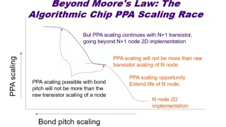
Global – October 25, 2026 -- A May 2026 "Tau Scaling Law" announcement claims production deployment of design-driven chip scaling across hundreds of chip variants over six years. That claim turns algorithmic power, performance and area (PPA) gains from a research topic into a commercial benchmark for EDA vendors and foundries, according to an industry analysis.

Tau framework targets signal delay instead of transistor size

The announcement was covered by Reuters, CNBC, Nikkei Asia, Forbes and The Register. It reframes scaling around time delay rather than geometry. The goal is to cut delay across devices, interconnects, circuits, chips, software and systems through architecture, placement, routing, 3D integration and hardware/software co-optimization.

Aspocomp Gives Every PCB Customer a Dedicated Contact at Oulu Plant

Image
Aspocomp Gives Every PCB Customer a Dedicated Contact at Oulu Plant

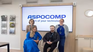
Oulu – October 24, 2026 -- Aspocomp assigns every printed circuit board (PCB) customer a dedicated contact person, handled by a customer service team based at the company's Oulu factory.

Single contact handles each order from quotation to shipment

The team receives requests for quotation (RFQs), prepares offers, processes orders and tracks them until the boards ship. "From the customer's perspective, we are often the main contact point," said Maria Pasanen of the customer service team.

The team coordinates with sales, production and technical experts. It also monitors schedules and checks that documentation and specifications are handled correctly. Once the finished PCBs are ready, it notifies the customer that the delivery is on its way.

Aspocomp Hires 14-Year PCB Veteran to Lead Central Europe Sales

Image
Aspocomp Hires 14-Year PCB Veteran to Lead Central Europe Sales

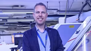
Oulu – October 24, 2026 -- Aspocomp has appointed Dominic Büch, a PCB industry professional with 14 years of experience, as Sales Manager for Central Europe, with a focus on defence and semiconductor customers.

Büch moves from product management to key account sales

Büch previously worked as Product Manager for HDI and wire bonding. He later became Key Account Manager for global electronics manufacturers. At Aspocomp he is responsible for technical sales and customer relationships across Central Europe.

Defence and semiconductor sectors drive demand for technical PCB support

Büch says customers in both sectors are actively seeking reliable, high-performance PCB partners. Early involvement is central to his approach: Aspocomp flags manufacturability issues and material risks during the layout phase to help customers avoid costly iterations.

Aspocomp adds two 6-spindle drilling machines to expand PCB capacity

Image
Aspocomp adds two 6-spindle drilling machines to expand PCB capacity

Finland – October 24, 2026 -- Aspocomp has invested in two new 6-spindle drilling machines to expand its drilling capacity and technology capabilities for high-reliability printed circuit boards (PCBs). The company describes the units as best-in-class equipment currently available on the market.

Drilling creates the electrical interconnections between PCB layers. Aspocomp says the accuracy, stability and consistency of this step directly affect signal integrity, reliability and overall product performance.

Backdrilling and high aspect ratio drilling are the headline capabilities

Aspocomp lists the following focus capabilities for the new platform:

GF Maps Cloud-to-Edge Chip Portfolio for AI Workloads

Image
GF Maps Cloud-to-Edge Chip Portfolio for AI Workloads

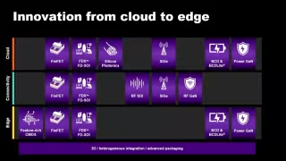
Global – October 22, 2026 -- GF has laid out a cloud-to-edge portfolio of essential chips for AI, spanning silicon photonics, power delivery, advanced packaging, RF, embedded memory and low-power compute, in a talk at CEA-LETI.

The company ties the portfolio to AI use cases in autonomous driving, healthcare, robotics and industrial automation.

GF targets GPU connectivity and data center power in the cloud

Connecting more GPUs for more powerful AI models requires higher data rates, which GF addresses with Fotonix silicon photonics and optical networking.

For data centers seeking sustainable power and lower CO2 emissions, GF points to GaN, BCDLite and FinFET technologies. They provide low transmission loss power delivery and fast transient response voltage regulation.