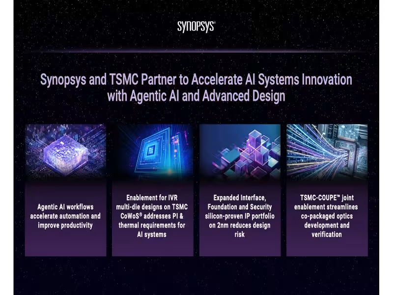
Sunnyvale, Calif. – September 23, 2026 -- Synopsys (Nasdaq: SNPS) has certified its EDA flows on TSMC's A14 process node and expanded a multi-die design collaboration covering agentic AI workflows, integrated voltage regulators on CoWoS® packaging, and co-packaged optics support for TSMC's COUPETM technology.
A14 certification covers digital and analog flows for next-generation chip designs
Synopsys said its certified flows now span implementation through signoff on TSMC's A14 node, including a new device routing enablement milestone for analog place-and-route automation. The companies frame the milestone as critical to speeding customer adoption of advanced process technology for AI and HPC applications.
Agentic AI tools automate floorplanning and layout tasks across design workflows
Synopsys Custom CompilerTM now accelerates analog migration, while Fusion CompilerTM applies LLM-assisted analysis to digital design productivity. A new agentic AI chiplet floorplan co-optimization flow built on the Synopsys 3DIC Compiler platform automates complex floorplanning for multi-die designs supporting TSMC 3DFabric® technologies.
3DIC Compiler platform adds unified co-design for IVR on CoWoS packaging
To address power delivery demands in AI systems, Synopsys 3DIC Compiler now enables designers to co-design and simulate integrated voltage regulators (IVRs) on TSMC CoWoS® technology within a single environment, targeting power integrity and thermal management for advanced packaging.
Photonic-electronic co-design flow targets TSMC COUPE optical interconnects
Synopsys continues joint enablement for co-packaged optics on TSMC's COUPETM technology, offering an integrated flow spanning 3DIC implementation, multiphysics analysis, and optimization to help customers verify optical interconnect architectures for multi-die systems.
N2P tape-outs deliver PCIe 7.0, HBM4, and 224G Ethernet PHY IP for AI workloads
On TSMC's N2P process, Synopsys achieved IP enablement and tape-out milestones including PCIe 7.0, HBM4, LPDDR6/5X/5, 224G Ethernet PHY, UCIe, OTP, and Silicon Lifecycle Management PVT monitoring IP. The company said these solutions address high-bandwidth connectivity and memory performance requirements for AI workloads, building on prior first-silicon success across TSMC's N5, N3P, and N2P nodes.
UCIe-A silicon demonstration validates die-to-die connectivity on N3P test chip
Synopsys demonstrated UCIe-A 32G/40G silicon on a TSMC N3P test chip integrated with a CoWoS-S interposer, validating high-speed die-to-die connectivity for AI systems. The company has also completed 64G UCIe IP tape-outs on both 2nm and 3nm nodes, with embedded DFT capabilities for in-system visibility.
"Our joint innovations with TSMC address the continuum of silicon to systems co-design capabilities needed to accelerate development of next-generation AI and high-performance computing systems," said Michael Buehler-Garcia, Senior Vice President at Synopsys.
Synopsys also expanded its Foundation, MIPI, and memory IP portfolio for TSMC's N3P and N2P nodes and is developing IP on compact process technologies spanning 6nm through 3nm, targeting data center, networking, mobile, automotive, and edge AI applications.